Key takeaways
- Advanced chip packaging joins chip parts in smarter ways, not just on one flat piece.
- It matters because AI chips need huge speed, high memory, and lower power use.
- Big chip firms now treat packaging as a core technology, not a final wrapping step.
- Methods like 2.5D, 3D, and chiplets help companies build bigger chips without making one giant slab.
- Packaging bottlenecks can slow AI supply, even when chip design is ready.
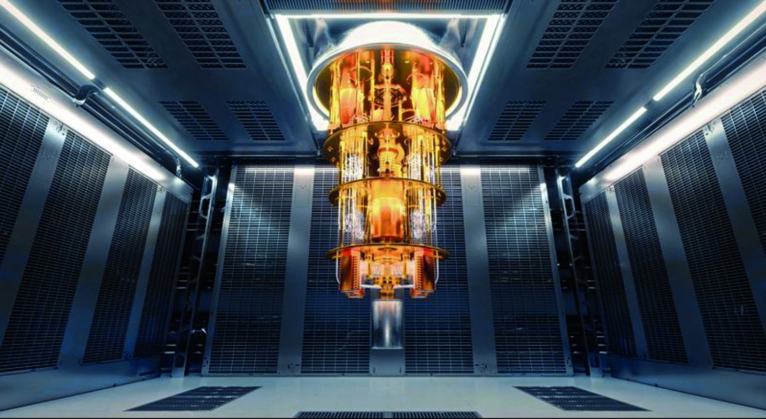
Advanced chip packaging is a new way to connect chip parts very closely. Advanced chip packaging means stacking or linking small pieces so they act like one powerful brain. That helps AI chips move data faster. It also helps them save space and power.
What is advanced chip packaging?
For years, chipmakers built most chips as one big piece of silicon. Silicon is the base material inside most chips. Then they put that chip in a package, which is the protective shell and connection layer.
Now that old method is hitting limits, because AI chips need much more from a tiny space. So companies are changing the package itself into part of the performance plan. That is why advanced chip packaging matters so much today.
In simple terms, it lets firms place several chip blocks side by side or on top of each other. Those blocks can include logic, which does the computing work, and memory, which stores data for fast access. The parts sit much closer together than before.
That closeness matters a lot. Data has a shorter distance to travel, so the chip can respond faster. It can also waste less energy as heat. For AI systems, that can mean more work done every second.
Why is advanced chip packaging suddenly crucial for AI?
AI models are huge, and they chew through massive amounts of data. A model is the trained system that spots patterns and gives answers. To keep up, AI chips need fast links between computing parts and memory.
Older chip designs struggle here. You can keep making transistors smaller, but gains are harder to get now. Transistors are tiny switches inside chips. So the industry is looking beyond just shrinking parts.
That is where advanced chip packaging comes in. It helps chipmakers mix many smaller dies into one system. A die is one cut piece of processed silicon. Instead of one monster chip, companies can use several smaller ones.
This method can improve yield, too. Yield means how many good chips come out of a factory batch. If one giant chip has one defect, the whole thing may fail. But smaller chip parts can be easier and cheaper to produce.
AI also creates a heat problem. Powerful chips get very hot while training models and serving answers. So companies need designs that manage heat better while still packing in more performance. Packaging now helps with that balancing act.
How do 2.5D, 3D, and chiplets work?
You will often hear about 2.5D, 3D, and chiplets. They sound tricky, but the basic idea is simple. Each one brings chip parts closer together, so they can talk faster.
In 2.5D packaging, several chips sit side by side on a base layer called an interposer. An interposer is a thin platform that links the chips. This can connect logic chips with high-bandwidth memory, or HBM. HBM is very fast memory stacked in layers.
In 3D packaging, chips are stacked vertically. Think of books piled on a desk instead of spread across the floor. That saves space and can cut the distance data must travel.
Chiplets are another big idea in advanced chip packaging. A chiplet is a small chip block built for one job. One chiplet may handle computing, while another handles memory or input and output.
Because of that, firms can mix and match parts like building blocks. They can also update one block without redesigning everything. That can save time, money, and factory capacity.
Why advanced packaging helps AI chipsSpeedMemoryPower saveHighHigherHighest
Who is leading the advanced chip packaging race?
Some of the biggest names in chips are pushing hard here. TSMC, Intel, Samsung, Nvidia, AMD, and Apple all care deeply about packaging. TSMC is Taiwan Semiconductor Manufacturing Company, the world’s largest contract chipmaker.
Nvidia’s AI chips, for example, rely on tight links between computing units and HBM. AMD also uses chiplets in several products. Intel has promoted its own packaging methods, while Samsung is investing in similar tools.
This race is not only about design anymore. It is also about who can manufacture these complex packages at scale. Scale means making large volumes reliably and on time.
That is one reason supply can get tight. Even when chip demand is huge, packaging lines may still be limited. As a result, the package can become the bottleneck, or the slowest point in supply.
What do the numbers show?
The AI boom has pushed demand for advanced manufacturing across the chip chain. One AI accelerator can cost thousands of dollars, while the systems holding many chips can cost far more. That puts intense value on every step that improves performance.
HBM is a clear example. Each HBM stack can include 8, 12, or even more memory layers. Those layers sit close to the main processor, because AI work needs very fast data access.
Modern AI servers can use 8 chips in one tray, and many trays in one rack. A rack is the tall cabinet that holds computing gear. So even a small gain in power use or data speed can matter at a huge scale.
| Term | What it means | Why AI cares |
|---|---|---|
| Chiplet | Small chip block with one main job | Lets firms build big systems from smaller parts |
| 2.5D | Chips placed side by side on a linking base | Helps processors sit near fast memory |
| 3D | Chips stacked on top of each other | Saves space and shortens data travel |
| HBM | Stacked high-speed memory | Feeds AI chips data very quickly |
Why does this matter for India and the chip industry?
India wants a bigger role in semiconductors, so this shift is worth watching closely. Semiconductors are the tiny electronic parts that power phones, cars, and data centers. Packaging is one area where countries can build useful strength faster than cutting-edge chip fabrication.
That does not make packaging easy. It still needs clean factories, precision tools, and deep engineering skill. But it can open a practical path into the global chip supply chain.
We have already seen India push hard on chip policy in stories like India Semiconductor Mission 2.0. We also covered how electronics firms are moving into richer work in Dixon’s speciality EMS move. Packaging fits into that bigger picture.
There is also a money angle. If packaging becomes a chokepoint, companies that solve it can gain pricing power and strategic value. That is similar to how critical infrastructure matters in sectors like ports and logistics funding or in fast-moving digital rails like mobile-first netbanking.
What is the big takeaway on advanced chip packaging?
Here is the simple answer: advanced chip packaging is no longer the box around the chip. It is part of the chip’s brain, speed, and efficiency. That is why the technology has become crucial for AI.
As chip shrinking gets harder, packaging offers a new road forward. It lets companies join memory and computing more tightly. It also helps them build larger AI systems without betting everything on one giant chip.
That is the quotable core of this story:
Advanced chip packaging is the method that turns several chip pieces into one faster, denser, and more power-efficient AI system.
For readers who want the source background, see CNBC TV18’s report and primary company material from TSMC and Intel.
FAQs
What is advanced chip packaging in simple words?
It is a way to connect small chip parts very closely. That helps them act like one stronger chip.
Why does AI need advanced chip packaging?
AI chips must move huge amounts of data fast. Packaging helps memory and computing stay close, so speed rises and power waste falls.
Who uses advanced chip packaging today?
Major chip companies do, including Nvidia, AMD, Intel, Samsung, Apple, and TSMC. They use it for AI, phones, and high-end computing.