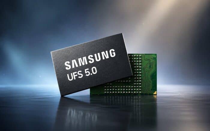
Samsung Electronics has officially announced the development of the industry’s first Universal Flash Storage (UFS) 5.0 solution, obliterating previous mobile memory speed barriers to accommodate the intense data demands of the on-device AI era.
By integrating the latest JEDEC embedded memory interface standards, the chip achieves data transfer speeds that mirror high-end laptop PCIe SSDs rather than traditional phone storage.
1. The Speed Profile: Doubling the Ceiling
The core upgrade of UFS 5.0 is an unprecedented leap in sequential data processing, effectively doubling the bandwidth of the previous UFS 4.1 standard:
- Sequential Read Speed: Up to 10.8 GB/s (Gigabytes per second).
- Sequential Write Speed: Up to 9.5 GB/s.
- The Baseline Comparison: For context, the UFS 4.1 chips powering today’s top-tier flagships max out around 4.3 GB/s read and 4.0 GB/s write.
2. Transforming Storage into an AI Component
Historically, smartphone flash storage was treated as a passive vault to hold photos, videos, and apps. However, as generative AI rapidly migrates from the cloud to local hardware, storage latency has become a major system bottleneck.
[On-Device AI Request] ──► UFS 5.0 Flash Asset (10.8 GB/s Read) ──► Instant LLM Weight Loading ──► Near-Zero Latency Output
Running large language models (LLMs) locally requires massive data sets to be fetched and fed into the phone’s NPU/compute engines continuously. UFS 5.0 acts as a high-speed pipeline, drastically cutting down model-loading latency and delivering near-instant response times for on-device AI features.
3. Physical Footprint and Power Efficiency
Despite the exponential performance gains, Samsung heavily optimized the silicon for small, battery-constrained devices using custom clock gating and multi-voltage technologies:
- ⚡ 40% Power Reduction: The memory architecture utilizes over 40% less power than UFS 4.1 to transfer the exact same volume of data, directly extending device battery life during heavy computing cycles.
- 📐 16.7% Smaller Package: The physical chip package measures just 7.5mm × 13mm × 0.9mm. Shrinking the storage footprint gives hardware engineers far greater internal design flexibility to pack larger batteries or advanced thermal cooling systems into future devices.
4. Production Window & Device Target
Samsung plans to initiate mass production of the UFS 5.0 chips in the fourth quarter of 2026 (Q4 2026).
The storage modules will launch in a variety of storage configurations topping out at 1TB capacities. Given the backend launch timeline, industry analysts expect UFS 5.0 to make its commercial debut in next-generation flagship smartphone lineups, premium extended reality (XR) headsets, and standalone AI wearables arriving in early 2027.