In a decisive step away from basic device assembly and toward deep component fabrication, India is poised to save approximately ₹40,000 crore annually in foreign exchange by transitioning to domestic Printed Circuit Board (PCB) production.
The announcement was made by Union Electronics and IT Minister Ashwini Vaishnaw during a joint foundation-laying ceremony with Uttar Pradesh Chief Minister Yogi Adityanath. The event marked the launch of high-end manufacturing units within the new 206-acre Electronics Manufacturing Cluster (EMC) near the upcoming Jewar Airport in the Yamuna Expressway region (YEIDA), Uttar Pradesh.
1. Shifting from Assembly to “Deep Manufacturing”
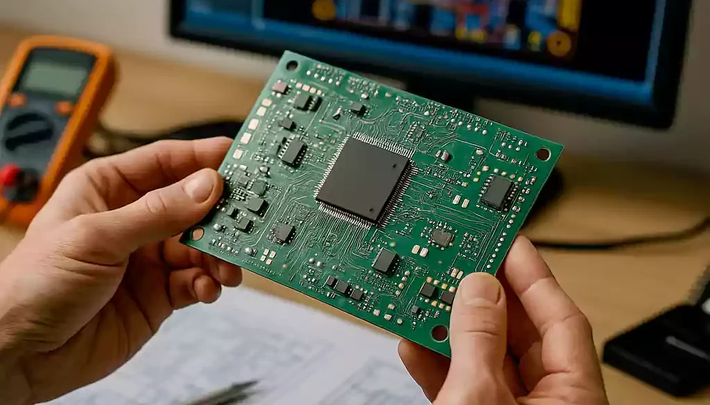
Printed Circuit Boards are the essential structural backbone of all modern technology, providing the physical foundation and intricate electrical pathways that allow chips and delicate resistors to communicate.
Historically, while India rapidly scaled up mobile phone and laptop assembly, it remained heavily dependent on importing the actual underlying multi-layer circuit boards—primarily from China and Taiwan.
- The Layer Revolution: The new domestic facilities are designed to manufacture highly sophisticated, advanced multi-layer PCBs (some featuring 20 to 22 layers of integrated circuitry compressed into razor-thin boards).
- The Import Substitution: By localized sourcing of these complex substrates, Indian device manufacturers can erase the massive ₹40,000 crore import bill, keeping that capital circulating within the domestic economy while building an end-to-end local hardware supply chain.
 [ Historical Loop ] ──► Import 20-Layer PCBs ──► Assemble Devices in India ──► ₹40,000 Cr Outflow
                                                                                   │
                                                                                   ▼ (Jewar EMC 2026 Shift)
 [ Local Supply Chain] ──► Manufacture Complex PCBs ──► High-Value Local Integration ──► ₹40,000 Cr Saved
2. Anchor Investments and Infrastructure
The financial milestone is anchored by major private and public industrial commitments that are turning the Jewar industrial belt into a premier global electronics zone:
- The Amber-Korea Circuit JV: Leading Indian contract manufacturer Amber Enterprises has formed a high-profile ₹3,250 crore joint venture with South Korea’s Korea Circuit Co. Ltd. (KCC). This factory will focus entirely on producing High-Density Interconnect (HDI) PCBs, flexible PCBs, and advanced semiconductor substrates.
- The Ancillary Eco-Hub: Amber is setting up an additional, standalone ₹3,500 crore facility across 100 acres nearby to manufacture core inputs like copper-clad laminates and localized components for commercial room air conditioners.
- Green Manufacturing Infrastructure: Both mega-plants are strictly engineered as Zero Liquid Discharge (ZLD) facilities, featuring closed-loop water recycling networks to minimize industrial waste runoff. Together, they are projected to instantly generate 3,000 direct, high-skilled engineering jobs.
3. The Wider Policy Tailwinds
The ₹40,000 crore saving directly aligns with a heavy, multi-billion-dollar policy pivot executed by the Central Government to turn India into the world’s second-largest electronics exporter:
| Active Government Program | Fiscal Structure & Scope | Explicit Focus Area |
| Electronics Components Manufacturing Scheme (ECMS) | Outlay scaled to ₹40,000 crore under the recent Union Budget. | To incentivize the heavy capital expenditure required to forge multi-layer PCBs, camera modules, oscillators, and sub-assemblies. |
| Modified Electronics Manufacturing Clusters (EMC 2.0) | Developed via a ₹417 crore budget (with a ₹144 crore direct Central grant). | Providing ready-to-use industrial plots, plug-and-play factory sheds, and shared amenities to speed up setting up plants. |
| India Semiconductor Mission 2.0 | Comprehensive multi-year sovereign backing. | Scaling past raw component assembly to support local raw material chemical processing, domestic IP design, and silicon packaging. |
By building out the complex lithography and lamination infrastructure needed for high-density PCBs right at home, India is systematically removing its biggest electronics supply chain vulnerability, paving the way for complete hardware self-reliance heading into 2027.