
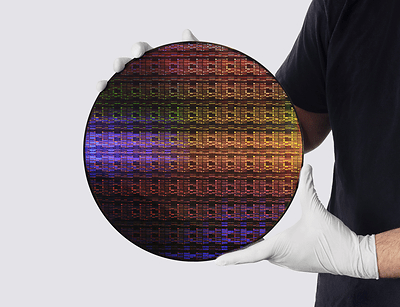
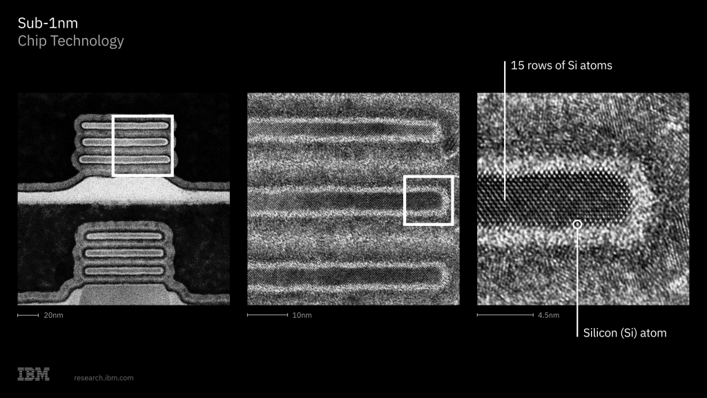
In a monumental milestone for the semiconductor industry, IBM has officially unveiled the world’s first sub-1 nanometer (nm) chip technology.
The historic breakthrough introduces a working architecture at the 0.7 nm node—equivalent to 7 angstroms—effectively pushing silicon engineering beyond the traditional nanometer scale down to the realm of individual atoms.
1. Pushing Past the Boundaries of Silicon
As traditional microchip design hits severe physical and thermal limits, shrinking transistors the old-fashioned way has become nearly impossible. IBM’s 0.7 nm process circumvents this bottleneck not just by scaling horizontally, but by rewriting how components occupy physical space:
- The Fingernail Metric: The breakthrough design allows engineers to pack an astonishing 100 billion transistors onto a slice of silicon roughly the size of a human fingernail.
- Doubling the Density: This represents nearly twice the transistor density of IBM’s own milestone 2 nm chip, which shook the hardware industry when it was introduced back in 2021.
- The Atomic Scale: To put 7 angstroms into perspective, a single human red blood cell is roughly 7,000 nanometers wide—making it 10,000 times larger than one of these atomic-scale nodes.
                      [ Transistor Density Evolution Matrix ]

  2021 (IBM 2nm Node)   ███████████████ ~50 Billion Transistors

  2026 (IBM 0.7nm Node) ██████████████████████████████  ~100 Billion Transistors (Fingernail Size)
2. The Innovation Engine: “Nanostack” 3D Architecture
The secret behind achieving sub-1nm performance without causing severe electrical leakage or computational “noise” lies in a brand-new transistor blueprint called Nanostack.
Developed at IBM’s global R&D hub in Albany, New York, in coordination with ecosystem partners like ASML and Lam Research, Nanostack moves away from monolithic single-layer printing. Instead, it utilizes 3D sequential integration to vertically stack and stagger nanosheet transistors on top of one another like a minuscule, high-tech city.
Crucially, this vertical layering allows chip designers to mix and match entirely different chemical material combinations inside each independent stacked layer, maximizing individual transistor efficiency. Furthermore, technical data presented at the VLSI 2026 symposium demonstrated that Nanostack achieves a 40% scaling efficiency boost in SRAM, providing the high-bandwidth data channels desperately required by next-generation artificial intelligence workloads.
3. Anticipated Performance Metrics & Timeline
According to IBM’s published research data, transitioning from the current state-of-the-art 2 nm baseline to the new 0.7 nm architecture yields massive performance and sustainability upgrades:
| Metric Vector | Projected Sub-1nm Breakthrough vs. 2nm Baseline |
| Pure Processing Performance | Up to 50% greater computing speed at identical power thresholds. |
| Energy Consumption Efficiency | Up to 70% reduction in power usage when running identical workloads. |
| Commercial Roadmap | IBM has established a viable manufacturing path to bring Nanostack into commercial foundry production within the next 5 years. |
The practical real-world implications are massive. For hyperscale data centers running massive large language models, a 70% reduction in power consumption could radically curb the global energy crisis fueled by the AI boom. For consumer electronics, it translates to smartphones and laptops that could operate for days or weeks on a single charge while executing heavy, on-device agentic AI models with zero latency.