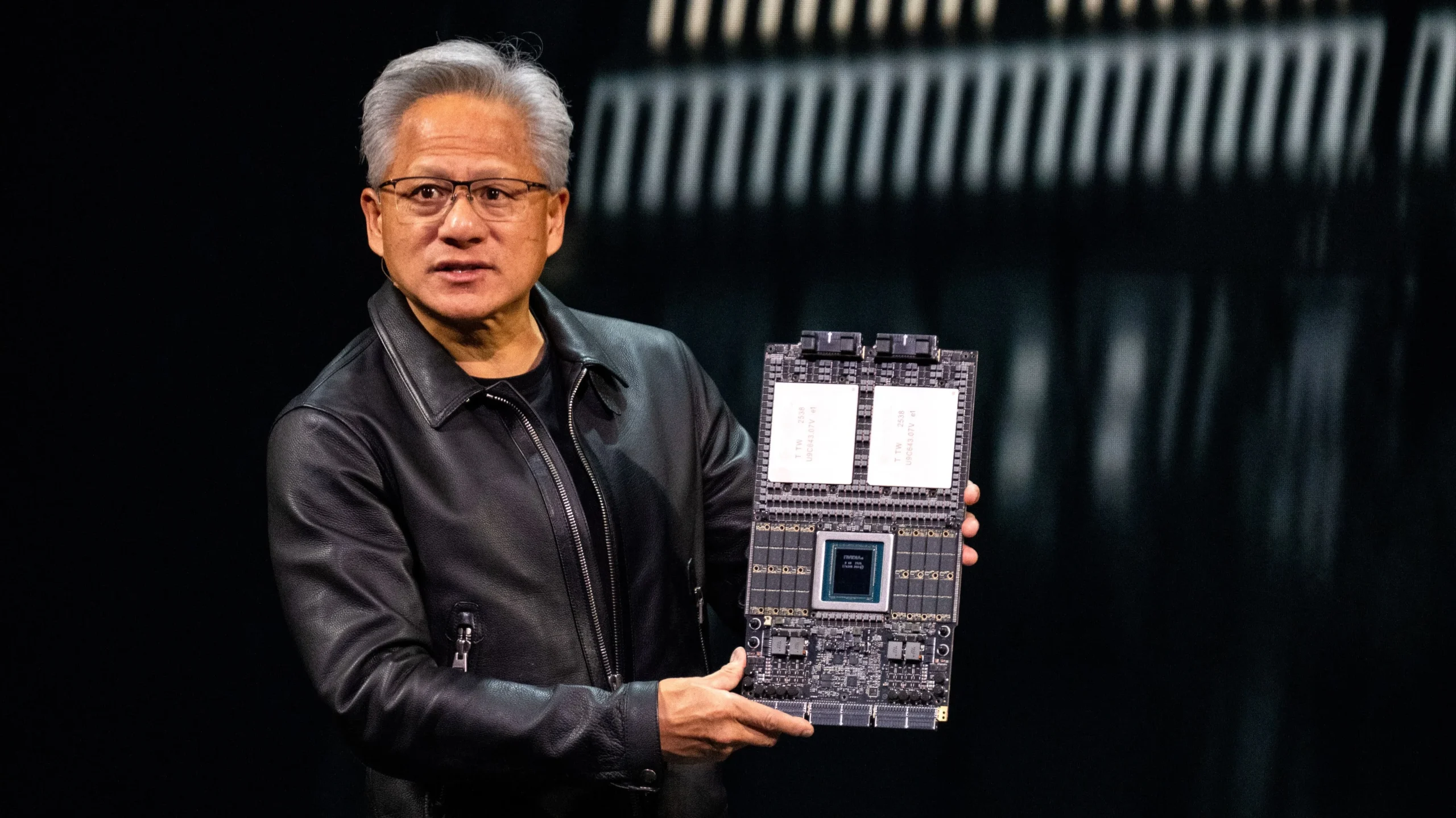
NVIDIA’s aggressive annual hardware roadmap has hit a major speed bump. According to a detailed report released today, July 6, 2026, by semiconductor research firm SemiAnalysis, NVIDIA’s highly anticipated Kyber NVL144 rack-scale architecture has been officially delayed to 2028.
The next-gen system, which Jensen Huang personally unveiled just three months ago at GTC 2026, was originally slated to debut in 2027 to power the company’s marquee Rubin Ultra AI chips. The 12+ month postponement has triggered a broader wave of product cancellations and structural changes to NVIDIA’s scaling timeline.
1. The Bottleneck: The 78-Layer PCB Midplane
The primary culprit behind the year-long delay isn’t the silicon chips themselves, but a massive physical engineering constraint in the server cabinet’s backplane.
To achieve ultra-high density and eliminate miles of traditional copper cabling, the Kyber architecture relies on an orthogonal midplane. Compute trays are slid in vertically from the front, plugging at a strict 90-degree angle directly into vertically mounted NVLink Switch blades at the back.
- The Manufacturing Wall: This specialized printed circuit board (PCB) midplane requires laminating three separate 26-layer boards into a single 78-layer monster.
- Signal Integrity Failure: To handle the lightning-fast 448G+ signal requirements of the Rubin Ultra generation, the board uses bleeding-edge quartz fabric (Q-fabric) and PTFE materials with trace widths under 25 micrometers. Fabricators are currently hitting severe yield walls, making the component functionally impossible to mass-produce at scale in 2026/2027.
2. Collateral Cancellations & Scope Reductions
The midplane manufacturing crisis has forced NVIDIA to radically scale back its near-term networking ambition for Rubin Ultra:
- NVL72x2 Scrapped: NVIDIA had planned a “back-to-back” dual-rack architecture to bridge 144 GPUs smoothly. This has been canceled outright after major cloud service providers (CSPs) and hyperscalers heavily rejected the awkward design and high operational burdens.
- NVL576 Constrained: The massive scale-out system meant to link eight individual racks via Co-Packaged Optics (CPO) is either delayed indefinitely or restricted to ultra-low-volume experimental builds, as CPO tech isn’t expected to fully mature until the subsequent Feynman platform.
- Rubin Ultra Silicon Dialed Down: This follows separate reports from late June indicating that the high-end 4-chip version of the Rubin Ultra processor was quietly downscaled to a dual-chip configuration because TSMC’s advanced CoWoS-L packaging couldn’t reliably execute multi-reticle scaling.
3. What This Means for the AI Hardware Landscape
| The Impact Point | The Reality for Infrastructure Teams |
| Capacity Planning Shift | Big Tech hyperscalers (Meta, Microsoft, AWS, Google) will have to rely on Blackwell Ultra architectures significantly longer than their 2027 roadmaps anticipated. |
| The Scalability Gap | Without the Kyber NVL144 domain working seamlessly, NVIDIA currently lacks a validated, monolithic architecture to scale out mega-clusters for training next-gen frontier models in 2027. |
| A Competitive Window | This delay hands a prime architectural window to AMD (with its upcoming MI500X platform) and Google (with TPUv8i Broadfly) to capture high-end market share if their custom optical and cluster scaling solutions prove more reliable. |
The Big Takeaway: This delay underscores a growing theme in hardware circles—NVIDIA’s furious, self-imposed annual release schedule is no longer just fighting physics on the silicon die; it is colliding violently with the mechanical limits of power delivery, packaging, and basic circuit board fabrication.
Get the day’s top stories in your inbox
One concise email. No spam, unsubscribe anytime.