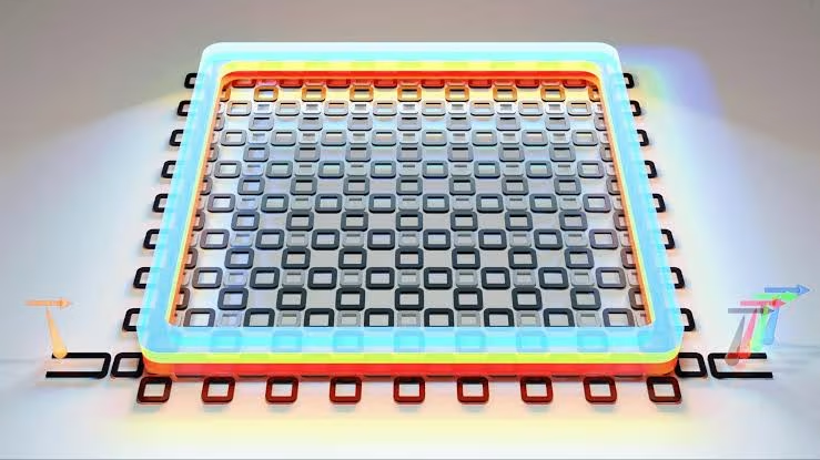
3D optical chip research just took a big leap forward. An optical chip is a chip that uses light, not only electricity, to move and handle information. A research team in China says it has cut production time from hours to seconds, a change that could make these light-based chips far easier and cheaper to build.
Key takeaways
- Researchers in China say they built a 3D optical chip far faster than earlier methods allowed.
- The team cut production time from hours to seconds by changing how the chip structures are formed.
- An optical chip uses light to carry signals, so it can be very fast and energy-saving.
- The advance is promising, but mass production still needs more testing and factory-scale proof.
What is a 3D optical chip, and why does it matter?
A 3D optical chip is built to guide light through tiny paths inside the chip. Those paths are called waveguides. A waveguide is a very small channel that steers light, much like rails guide a train.
Most normal chips move signals with electrons, which are tiny charged particles. An optical chip uses photons instead. Photons are particles of light, so they can move data very quickly and with less heat.
That matters because AI, data centres, and telecom networks need more speed each year. They also need to waste less power. Even small gains add up when thousands of servers run all day.
This is why labs around the world are chasing photonics. Photonics means technology that uses light. If these chips become easier to make, they could help computers talk faster inside machines and between machines.
What did the China team actually achieve?
According to the South China Morning Post report, the Chinese team said it cut fabrication time from hours to seconds. Fabrication means making the chip. That is a huge change in speed for any optical chip process.
The report points to a new way to create 3D structures inside optical material. Instead of a slow, step-by-step process, the team used a much faster method. The article suggests this could remove one of the biggest bottlenecks in making a 3D optical chip.
Think of it like building a toy city. The old method placed many tiny blocks one by one. The new method seems closer to stamping big parts almost at once.
Speed matters in factories because time is money. If one chip takes about 3 hours, a line can only make so many in a day. If the same step takes about 3 seconds, that is roughly 3,600 times faster, so output could jump sharply. The exact starting time may vary by setup, but the order of change is still striking, and that is why this news is drawing attention.
How could faster manufacturing change real technology?
A faster 3D optical chip process could help in several fields. One is AI hardware, which means the physical chips and machines that run AI models.
Another field is telecom gear, which carries internet and phone traffic. Light-based parts already do a lot of that work in fibre networks. A more advanced optical chip could make those systems smaller and quicker.
Medical devices may also benefit. Sensors that use light can spot tiny changes, so better chip designs could help tools that test blood, watch air quality, or scan materials.
There is also a data-centre angle. Big server buildings use a lot of electricity. If optical links cut heat and power use, companies save money and cooling gets easier.
Why are researchers moving toward 3D designs?
Many chips are mostly flat, like streets on a map. But a 3D optical chip can stack or cross light paths in more ways. That gives engineers more room to pack functions into a small space.
A simple 2D layout can run into traffic jams. Light paths may cross, and that creates design limits. A 3D design can route signals above, below, or around each other.
That extra freedom matters for complex systems. For example, chips for sensing or quantum work may need many tightly packed channels. More layers can help fit them in.
China is not alone in this race. Companies and labs in the US, Europe, and Asia are also pushing optical chip research. You can see related chip competition in our coverage of the Google Intel chip partnership for AI infrastructure and Alibaba’s AI stack challenge to Nvidia.
What are the catches before this reaches server rooms?
Fast lab results do not always become fast factory results. A prototype is an early test model. Companies still need to prove that the method works again and again, with very low defects.
That is the hard part. A defect is a flaw in the chip. Even tiny flaws can bend light the wrong way, so one bad spot may ruin performance.
Factories also care about yield. Yield means the share of chips that come out usable. A process can be quick, but if many chips fail, it may still be too costly.
Researchers must also show how well the chips perform after this fast build method. Can they handle heat? Do they keep signals clean? Can they scale from 10 devices to 10,000 devices?
| Point | Old approach | New report |
|---|---|---|
| Build time | Hours | Seconds |
| Possible benefit | Slower output | Much higher output |
| Main challenge | Time bottleneck | Need proof of yield and scale |
Why this optical chip story matters beyond China
This 3D optical chip story is not just about one lab. It shows how the chip race is widening beyond standard silicon processors. Silicon is the main material used in many chips today.
Countries want stronger positions in next-generation hardware. That includes AI chips, memory, sensors, and photonics. Each new method matters because it can shift who leads in future tech.
It also fits a larger pattern. Nations are trying to make more advanced parts at home. Meanwhile, businesses want faster tools for AI and cloud systems.
For readers, the plain answer is simple: if an optical chip can be made in seconds instead of hours, it could move from niche labs toward wider use much faster. That does not mean instant rollout, but it does mean the road just got shorter.
To see how hardware changes can affect the wider tech world, you can also read our explainer on Gemini rates and tracking AI use and our report on Google clicks and what they mean for website traffic.
The original report was published by the South China Morning Post. For basic background on photonics, readers can also check the Encyclopaedia Britannica explainer on photonics.
Frequently Asked Questions
What is a 3D optical chip?
A 3D optical chip is an optical chip that guides light through paths arranged in a three-dimensional design. It can move information very fast and may use less power than a standard electronic chip.
Why is cutting build time so important?
It matters because factories can make more chips in less time. The China team says it cut production from hours to seconds, which could lower cost and help optical chips move beyond small lab projects.
When could this reach real products?
That is still unclear. The team needs to show strong yield, reliability, and factory-scale production before wide commercial use of the optical chip begins.
Get the day’s top stories in your inbox
One concise email. No spam, unsubscribe anytime.