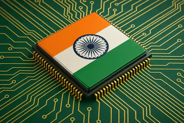
The Indian government is open to taking equity stakes in semiconductor design startups under the newly approved India Semiconductor Mission (ISM) 2.0, marking a major shift from the grant-based funding model used in the first phase of the program. Amitesh Kumar Sinha, CEO of the India Semiconductor Mission (ISM), said the Centre is willing to co-invest alongside private venture capital firms without seeking management control, aiming to attract more private capital into India’s fabless semiconductor ecosystem.
The proposal is part of Semicon 2.0, a ₹1.27 lakh crore initiative approved by the Union Cabinet to strengthen India’s semiconductor manufacturing, design, packaging, and supply chain capabilities. Under the new model, government funding will be milestone-based and structured as equity investments, with the Centre planning to exit its holdings as startups mature.
Centre Plans Equity Investments in Chip Design Startups
The new funding model is designed to encourage private investment while supporting promising semiconductor startups.
| Key Highlights | Details |
|---|---|
| Programme | India Semiconductor Mission (ISM) 2.0 |
| Government role | Equity co-investor |
| Focus | Semiconductor design startups |
| Investment approach | Match private VC investments |
| Management control | No operational control by government |
| Exit strategy | Government to divest as firms mature |
According to ISM CEO Amitesh Kumar Sinha, the government aims to reduce funding risks for investors while allowing founders to retain operational independence.
How the New Funding Model Works
Unlike Semicon 1.0, which primarily relied on grants, ISM 2.0 introduces a co-investment framework.
Key features include:
- Government will match eligible private investments.
- Funding will be linked to business milestones.
- Equity investments instead of one-time grants.
- No management or operational control by the Centre.
- Planned government exit after startups achieve scale.
- Greater participation from venture capital firms.
This structure is intended to create a more sustainable financing ecosystem for semiconductor startups.
Why the Policy Matters
India is looking to strengthen its position in the global semiconductor value chain.
The initiative seeks to:
- Encourage domestic chip design.
- Support fabless semiconductor companies.
- Attract global and domestic venture capital.
- Build intellectual property (IP) within India.
- Reduce dependence on imported semiconductor technologies.
- Create globally competitive chip startups.
India already has a significant semiconductor design talent pool, and policymakers want to translate that expertise into globally successful startups.
ISM 2.0: A Broader Semiconductor Push
| Area | Objective |
|---|---|
| Semiconductor design | Support fabless startups |
| Manufacturing | Expand domestic chip production |
| Packaging & testing | Strengthen ATMP/OSAT ecosystem |
| Capital | Mobilize private investment |
| Innovation | Build indigenous semiconductor IP |
The equity-investment model complements broader incentives under ISM 2.0 to develop India’s semiconductor ecosystem from design through manufacturing.
Benefits for Startups and Investors
The proposed framework offers several advantages.
Potential benefits include:
- Reduced funding risk for venture capital firms.
- Better access to growth capital.
- Long-term alignment between public and private investors.
- Greater confidence for early-stage semiconductor startups.
- Improved commercialization of chip designs.
By sharing financial risk, the government hopes to unlock more private investment in a capital-intensive sector.
Challenges Ahead
Despite the policy shift, several hurdles remain.
These include:
- Long product development cycles.
- High R&D costs.
- Limited domestic fabrication capacity.
- Global competition from established semiconductor hubs.
- Need for experienced semiconductor entrepreneurs.
- Scaling products from prototype to commercial production.
Addressing these challenges will be essential for building a globally competitive semiconductor ecosystem.
Outlook
The Centre’s willingness to take equity stakes in semiconductor design startups marks a significant evolution in India’s industrial policy. Rather than acting solely as a grant provider, the government is positioning itself as a catalytic investor that shares risk with private capital while allowing entrepreneurs to retain operational control. This approach could make India’s semiconductor startup ecosystem more attractive to venture capital firms and help accelerate the commercialization of indigenous chip designs.
If implemented successfully, the model could create a stronger pipeline of fabless semiconductor companies, complementing India’s investments in fabrication, packaging, and advanced manufacturing under ISM 2.0. Together, these initiatives are intended to strengthen India’s role in the global semiconductor supply chain and reduce dependence on imported technologies.
What It Means for India’s Semiconductor Industry
The proposed co-investment strategy reflects a broader shift toward market-driven public funding in strategic technology sectors. By matching venture capital investments rather than replacing them, the government aims to crowd in private investment while encouraging startups to remain commercially focused.
For India’s semiconductor industry, the move could accelerate the creation of homegrown intellectual property, strengthen the fabless chip ecosystem, and improve access to capital for early-stage innovators. Combined with manufacturing incentives under Semicon 2.0, the policy has the potential to support a more complete semiconductor value chain—from chip design and IP development to fabrication, packaging, and commercialization.
Get the day’s top stories in your inbox
One concise email. No spam, unsubscribe anytime.