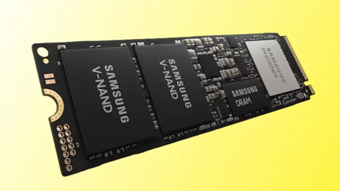


In a massive technological leap that pushes the semiconductor industry into the “thousand-layer era,” Samsung Electronics has successfully developed and verified the world’s first functioning 900-layer 3D V-NAND flash memory prototype.
The breakthrough nearly triples the density of any flash memory architecture currently in volume production. The milestone signals a disruptive shift in how the industry will scale dense, power-efficient storage infrastructure to cope with the global artificial intelligence data crunch.
The Architectural Shift: How Cell Multi-Bonding (CMB) Works
Historically, 3D NAND has been manufactured through a single-stack etching process—similar to drilling a continuous vertical shaft down through a multi-story apartment building from a single foundation. However, as vertical structures approach extreme heights, the microscopic drill path deflects, the layers misalign, and the entire silicon wafer begins to warp under accumulated stress.
To bypass this physical manufacturing wall, Samsung transitioned away from single-wafer etching to a highly advanced wafer-stacking architecture called Cell Multi-Bonding (CMB):
- The Twin-Tower Build: Instead of drilling 900 layers in one go, Samsung fabricates two separate 450-layer cell wafers up to their maximum reliable, high-yield heights.
- The Permanent Fuse: Using advanced hybrid bonding mechanisms, the backends of the two whole silicon wafers are precision-aligned and fused together using embedded metal bumps, transforming them into a unified 900-story integrated system.
Conventional Single-Stack          Samsung Cell Multi-Bonding (CMB)
       [ 400+ Layers ]                     [ 450-Layer Wafer ]
              |                                    || <-- Precision Hybrid Fused
       (Physical Limit:                            || <-- Metal Bumps
     Warping & Deflection)                 [ 450-Layer Wafer ]
                                                   = 900 Layers Integrated
Overcoming the Mechanical Hurdles
To transform this extreme stacking method into a functioning, real-world chip rather than a theoretical model, Samsung’s engineering teams had to design custom hardware overrides to tackle intense physical variables:
- Wafer Warpage: Stacking 450 layers creates massive material tension that distorts the silicon. Samsung resolved this by introducing a proprietary Upper Chuck Design, using specialized hardware clamps to keep the wafers completely flat during processing.
- Microscopic Misalignment: To line up billions of microscopic memory channels between the two independent wafers, the firm deployed newly developed Overlay Correction software to automatically adjust and map bonding points at the atomic level.
- Power Management: To prevent a 900-layer vertical stack from overheating or dropping voltage, Samsung redesigned its internal Bit Line (BL) and Word Line (WL) configurations, shrinking overall chip sizes while dropping power consumption per terabyte.
Leaving Competitors Behind in the AI Storage Race
The timing of the 900-layer prototype lands at a highly competitive juncture in the flash memory market. In current high-volume mass production, rival SK Hynix holds the layer-count crown with its 321-layer 4D NAND chips, while Chinese semiconductor champion YMTC has been aggressively shipping 232-layer and 294-layer alternatives at aggressive pricing tiers.
Samsung is currently preparing to ramp its 10th-generation V-NAND (V10)—which features a single-stack architecture of over 400 layers—toward commercial mass production in the second half of 2026. This new 900-layer prototype establishes a definitive “Super Gap” roadmap, proving the technical scalability of CMB and placing Samsung comfortably ahead on the path toward its ultimate goal of a 1,000-layer V-NAND module by 2030.
Why 900-Layer Silicon Matters for Enterprise and Edge AI
While regular consumers will eventually reap the benefits via high-capacity smartphones and client laptops, the immediate beneficiaries of this technology will be hyperscale cloud data centers.
Generative AI large language models (LLMs) require massive datasets that must remain continuously accessible. By vertically expanding storage capacity without changing the horizontal physical footprint (the die area) of the silicon, server operators can pack multi-terabyte architectures into single drive bays. Spreading fixed manufacturing costs across a significantly higher concentration of vertical bits allows data centers to drastically reduce cost-per-gigabyte, physical rack space, and overall cooling costs.