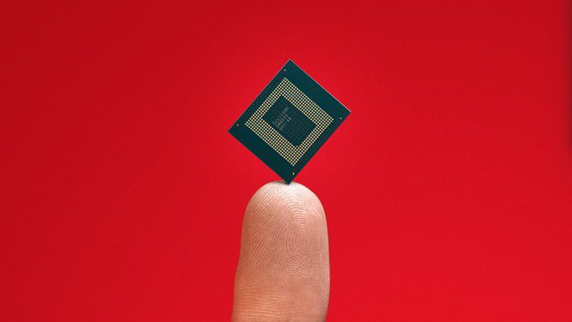
In a landmark development for India’s semiconductor ambitions, Renesas Electronics India Private Limited has inaugurated its first-ever 3-nanometer chip design centres in Noida and Bengaluru. These are the first centres in India specifically built to design chips at the 3 nm node, a cutting-edge scale of miniaturization that offers higher performance and energy efficiency. ETManufacturing.in
Key Details of the Launch
- The centres were inaugurated by Union Minister Ashwini Vaishnaw of Electronics & Information Technology. He emphasized that this move places India among the elite group of countries working on 3 nm design.
- The facilities have been set up by Renesas in two major tech hubs: Noida (Uttar Pradesh) and Bengaluru (Karnataka).
- The design centres are part of India’s broader semiconductor strategy, which includes design, fabrication, ATMP (Assembly, Testing, Marking and Packaging), and a full supply chain (including chemicals, gases, and equipment).
- As part of the effort, a semiconductor learning kit has been launched to enhance practical hardware skills among engineering students. Over 270 academic institutions that already have advanced Electronic Design Automation (EDA) software under the India Semiconductor Mission will receive these hardware kits.
Why 3 nm Matters & What This Enables
- Technology Leap: Moving from earlier nodes (e.g. 7 nm, 5 nm) to 3 nm involves much finer transistor scaling, allowing more transistors per unit area, lower power consumption, and improved performance. It’s essential for high-end, power-efficient chips needed in AI, automotive, IoT, etc.
- Global Competitive Position: Having domestic capability in designing 3 nm chips reduces reliance on foreign design centres, increases India’s technological sovereignty, and strengthens its place in the global semiconductor supply chain.
- Talent & Ecosystem Building: The learning kits, academic tools (EDA software, etc.), and startup engagement programmes aim to build a strong pipeline of engineers and innovators who understand both hardware and software aspects of advanced chip design.
Challenges & Next Steps
- Fabrication vs Design: Designing chips at 3 nm is one thing; fabrication (manufacturing) at that scale is far more demanding. India is still building that piece of the ecosystem. Ensuring partnerships or access to fabs and manufacturing foundries remains crucial.
- High Cost & Complexity: Advanced node design requires expensive tools, very specialized talent, rigorous validation, yield optimization, etc. Ensuring that the centres can deliver reliably is non-trivial.
- Supply Chain Bottlenecks: Chemicals, tool-chain components, gases, etc., needed for ultra-fine process nodes require global supply stability and regulatory clarity.
- Regulation, IP, and Security: With more sensitive chip design happening domestically, concerns around intellectual property protection, data security, and regulatory oversight will need attention.
Impacts & What to Expect
- Boost for Automotive, AI, Edge Devices: Companies designing chips or SoCs for automotive (infotainment, EV control systems, etc.), AI accelerators or edge devices will benefit from having a local, high-performance chip design base.
- Startup & Academic Innovation: With design centres and learning kits, more students and startups can prototype advanced chips or mixed signal / embedded designs, which could lead to indigenous IPs or products.
- Policy & Investment Leverage: The success of these centres could encourage more global semiconductor firms to invest in India, under schemes like PLI (Production Linked Incentive), Chips to Startup, and other incentives.
- Long-Term Goal toward Fabrication: Over time, if the ecosystem matures, it may make sense to have domestic fabs capable of manufacturing these designs — though that is a much larger investment and timeline.
Conclusion
The opening of Renesas’ 3 nm chip design centres in Noida and Bengaluru represents a landmark moment for India’s semiconductor journey. It demonstrates a strategic leap in capability, aligning with national goals of self-reliance and global competitiveness in high-tech fields. While design is only one part of the semiconductor value chain, this move lays important groundwork for future advancements, innovation, and ecosystem strength.


